Main menu
You are here
Perf+
[last updated: 2026-04-17]
Layout and Build Procedure:
LM317 voltage regulator project
Battery Interface Project
-----
- Boring Background/Overview:
- Bottom Line Assessment:
- Con: high learning curve for layout of bridges & cuts
Hopefully made easier by these notes... - Con: medium learning curve for soldering & cutting techniques
- Con: changes to circuit after it's built are much more difficult than with P2P wiring on a proto board.
- Pro: marginal improvement in assembly time vs. point-to-point wiring on a proto board,
that is, after the design and layout are done... - Pro: very tidy finished product
- Pro: very robust finished product:
As compared to standard solderless breadboards, in which it's difficult to avoid nicking the wires when you strip the insulation, even if ever so slightly. This becomes a weak point that will fatigue and break with even small amounts of bending/flexing (depending on how deep the nick is). The Perf+ avoids this completely.
Further, protoboard pin slots can be damaged with too-large diam wire, such that subsequent insertions of small wires don't make good contact. - Bottom Line: kind of a wash. Maybe comes down to personal preferences and values more than anything functional.
For me, the tidiness and robustness of finished product are important and swing the scale to the Perf+ for projects/circuits that are finalized and not likely to change after assembly. - Construction of the board:
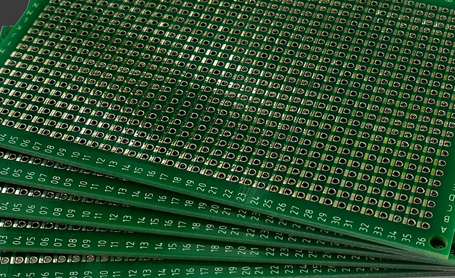
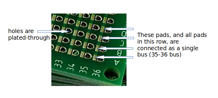
- The board is composed of plated-through holes.
Initially, each plated-through hole on the board is independent and Not connected to anything else. - On one side of the board, there are horizontal rows of bus lines.
On the other side of the board are vertical columns of bus lines.
The buses are composed of strings of connected pads, with a pad adjacent to each hole.
The horizontal bus pads in the same row are all connected to each other, and the vertical bus pads in a given column are likewise all connected to each other,
But the bus pads are NOT connected to the holes - until you manually solder them, ie. make a "bridge".
----------------------------------
- The board is composed of plated-through holes.
- Naming Convention:
- In order to keep track and make sense of what's going on, you must have a naming/numbering convention for the holes and buses.
It's arbitrary, and frankly I don't know if the mfr has defined it differently, but I'll follow this convention: - Holes:
- Hold the board with letters across the top, and numbers down the sides.
The letters should ascend from left-to-right, and the numbers ascend from top-to-bottom
If you have a complete, un-cut board, this will put A-01 in the top left corner.- Notice that, when the board is in this position, the pads for the horizontal bus that are on the side facing you
are very close to the holes, meaning those are the pads that you would bridge to (ie. between the pad and the plated-through hole)
in order to connect the hole to the horizontal bus. - The letters across the top now denote columns of holes, and the numbers on the sides denote rows of holes.
- A specific hole will be designated with "column-row."
- Define this as the "front" side of the board.
- Hold the board with letters across the top, and numbers down the sides.
- Buses:
- On the 'front' side of the board, buses run horizontally between each row of holes.
- On the back of the board, the buses run vertically between each column of holes.
- Horizontal buses on the front of the board will be designated with "row-row" to specify which two rows the bus lies between.
For example a given horizontal bus might be referred to as "05-06". - Vertical buses on the back of the board will be designated with "column-column" to specify which two columns the bus lies between.
For example a given vertical bus might be designated as "M-N".
----------------------------------
- In order to keep track and make sense of what's going on, you must have a naming/numbering convention for the holes and buses.
- How connections/bridges are made:
- Some holes are used to mount components. These holes must also have a bus connection (else the component will be 'floating' and unconnected to the circuit).
However some holes do not have components, but are only used to connect a horizontal trace on one side of the board to a vertical trace on the other side,
effectively creating a 90-deg "corner" in your circuit trace routing.
For such a corner hole, since you need to connect to both vertical and horizontal busses,
you need to make bus bridges on both sides of the board. - Make a bridge/bus-connection by putting a blob of solder between the hole and the bus pad adjacent to it.
- Some holes are used to mount components. These holes must also have a bus connection (else the component will be 'floating' and unconnected to the circuit).
- How cuts are made:
While it is doable to use an Exacto knife, it's a pain, IMO, so I highly recommend using a Dremel with a tiny burr grinding tip.
It's Much faster and Much cleaner.
Cut/grind on a bus line in between holes to remove the bus trace. - Layout and Build Procedure:
----------------------------------
.
.
.
eof

